Now that you have started taking interest in learning Verilog, it is necessary that we dive into the details of the Devil.
I’d begin explaining with the help of a Multiplexer module in Verilog.
Multiplexer:
We are well aware of the humble Multiplexer (MUX) that we have learnt in our Digital Design course. Just to brief it up, a MUX is a device that has n input lines, a select line, using which we get one output in the output line.
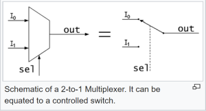 (Source : Wikipedia)
Now, when I would want to declare a MUX design – or from now, as we would term it – a module, we need to declare it using all it’s inputs and outputs. As we can see from the figure above, for a 2:1 MUX, we have 2 input signals, one select line (also an input) driving the MUX to give one output.
module mux (input wire [7:0] I1, input wire [7:0] I2, input wire sel, output reg [7:0] out); always @(a or b or sel) op = sel? I1 : I2 endmoduleFigure 1 : Module declaration using Verilog 2001
Family & Verilog:
Just to make things simpler, and clearer, let us study using the following analogy.
We know that a family is made up of its family members, in the same way – a hardware system is made up of its hardware elements or its family members. These family members are none other than the inputs and the outputs of the system.
Each of us has (had?) a nameplate outside our homes for easy identification of the members staying there. In the same way, in Verilog, whenever you declare a module (~family), we need to list down the names of all its family members (~inputs and outputs).
The type of declaration shown in Figure 1 is Verilog 2001 format which combines Port and Data type declaration. There is another format too, in you wish to look it up, can be found on the Internet.
Coming back to family, you can see wire and reg as certain datatypes. Signals which drive your system should be declared with wire datatype, while output of a system, or anything whose value we basically need to be stored, should be declared using reg.
Thumb rule#1 Think of signals in terms of wire and outputs in terms of reg.Taking another example of a Half-Adder:
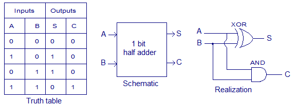
As seen from the block diagram above, A and B are the input to this system, while S and C are the output ports. Hence A and B will be declared as input wire while S and C as output reg.
The Verilog declaration of this design will be as follows:
Consider the example of a Full adder which uses 2 Half adders:
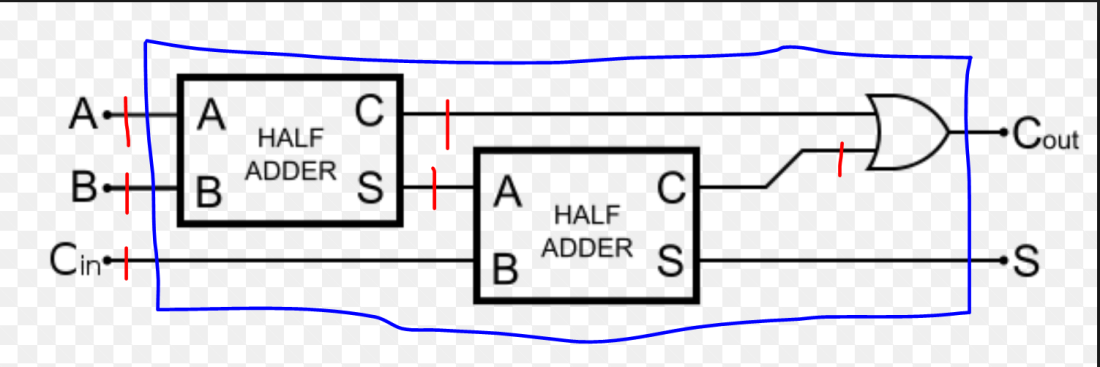
From the figure above, we can imagine Full adder’s internal block to be made of 2 half adders, and can easily realise that the inputs and outputs to this system are (A, B, Cin) and (Cout, S) respectively. However, inside the block, the wires marked in red, also drive some kind of information (or signals) from one end of the block to the other. And thus these internal signals should also be declared in your nameplate declaration. These internal signals are nothing but of wire datatype.
Combinational and Sequential Circuits:
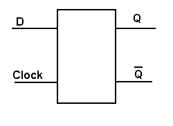
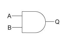
Take the above 2 basic examples of combinational and sequential circuit.
An AND gate will take the 2 inputs, and would almost immediately (with some inherent delay) transmit it to Q. While in the D flip flop, whatever the value is at D, would be available at Q only at some clock input.
This brings us to our Thumb rule#2
always block:
Sequential circuits involving reg comes under an always block.
As seen from the figure above, the always block has some parameters inside @().
This is nothing but the sensitivity list. A sensitivity list contains the inputs which on any change should trigger the block to execute.
Continue to Verilog 102 –
Advertisements Share this:


